


 CN


The PCB solder mask layer is a core functional protective layer of circuit boards. It provides insulation isolation, solder resist, corrosion resistance, and withstands high temperatures during reflow soldering, directly determining the long-term operational reliability of the board. Driven by AI computing power, high-speed optical modules, and other industries, demand for high-density, irregular-shaped, and customized PCBs continues to grow. Traditional liquid photoimageable (LPI), screen printing, and dry film solder mask processes are increasingly showing limitations in high-value-added scenarios such as ultra-fine circuits, thick copper boards, flexible boards, and small-batch prototyping: reliance on films or screen tooling, long process chains, complex wet-line operation and maintenance, long changeover times, and yield issues such as ink bleeding and residue during fine openings.
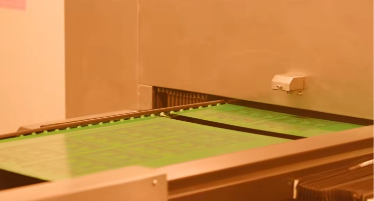
Hosonsoft PCB Solder Mask Ink Digital Inkjet Full-Stack Solution integrates self-developed boards, an inkjet control system, an optional vision alignment unit, a UV curing unit, and an industrial control host. It provides equipment OEM and system integrator with a rapidly integrable underlying technology base and opens an SDK for secondary development, helping industry partners advance the digital upgrade of PCB manufacturing and jointly explore new solder mask process routes.
I. Suitable for High-Value-Added PCB Manufacturing Scenarios
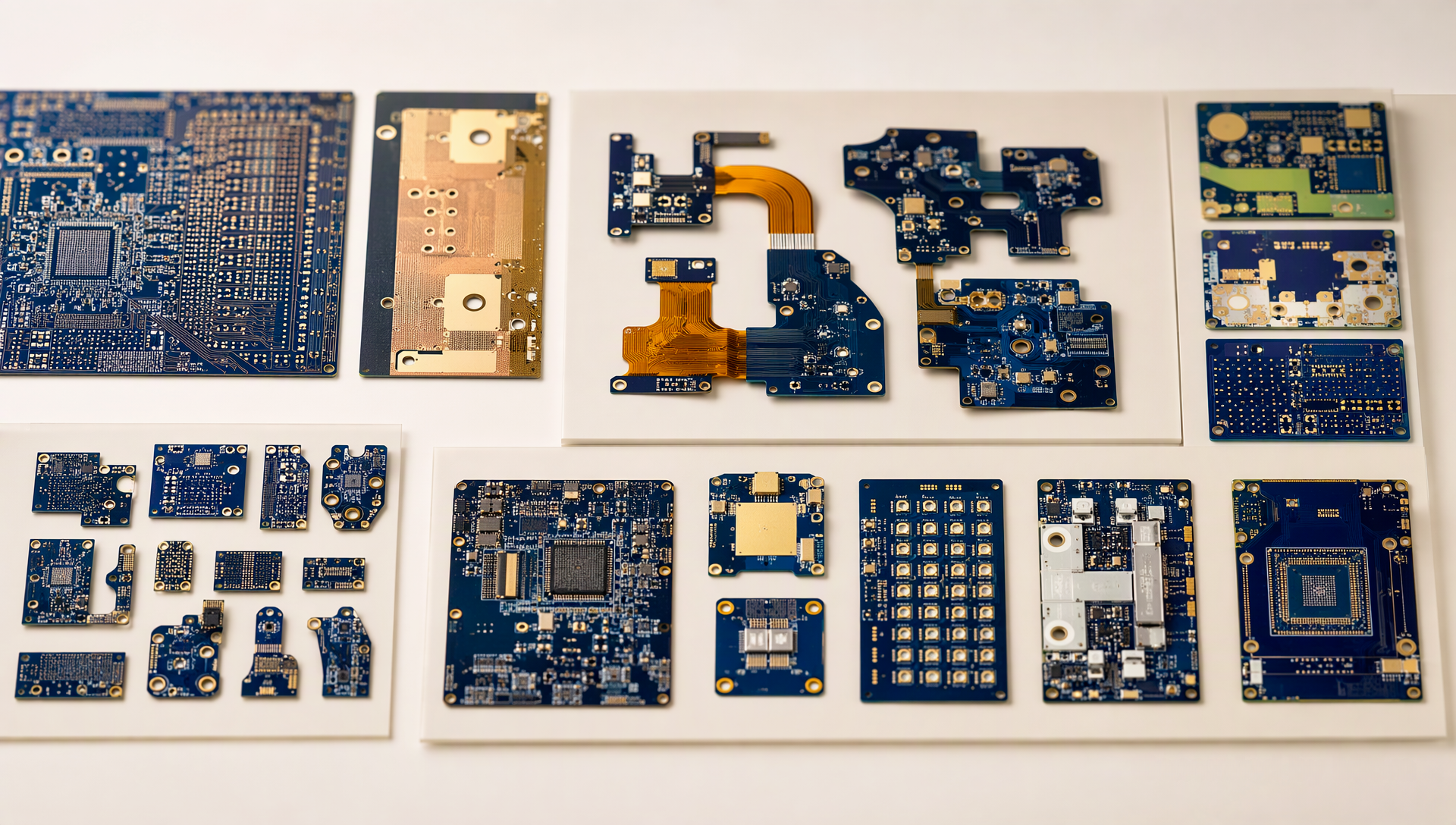
Hosonsoft PCB Solder Mask Ink Digital Inkjet Full-Stack Solution is suitable for high-value-added, high-process-difficulty PCB manufacturing requirements and covers multiple board types:
- HDI high-density circuit boards and fine-pitch precision circuit boards, thick copper boards, and ultra-thin substrate boards;
- Rigid-flex boards, FPC flexible circuit boards, and irregular-structure boards with height differences;
- R&D prototypes and multi-variety, small-batch rapid prototyping lines;
- Automotive electronics boards, RF boards, MiniLED backlight boards, power device boards, and packaging substrates;
- It also supports customized special process development such as zoned solder mask, local precise openings, and differentiated solder mask thickness control.
II. Applicable Focus of Different Solder Mask Processes
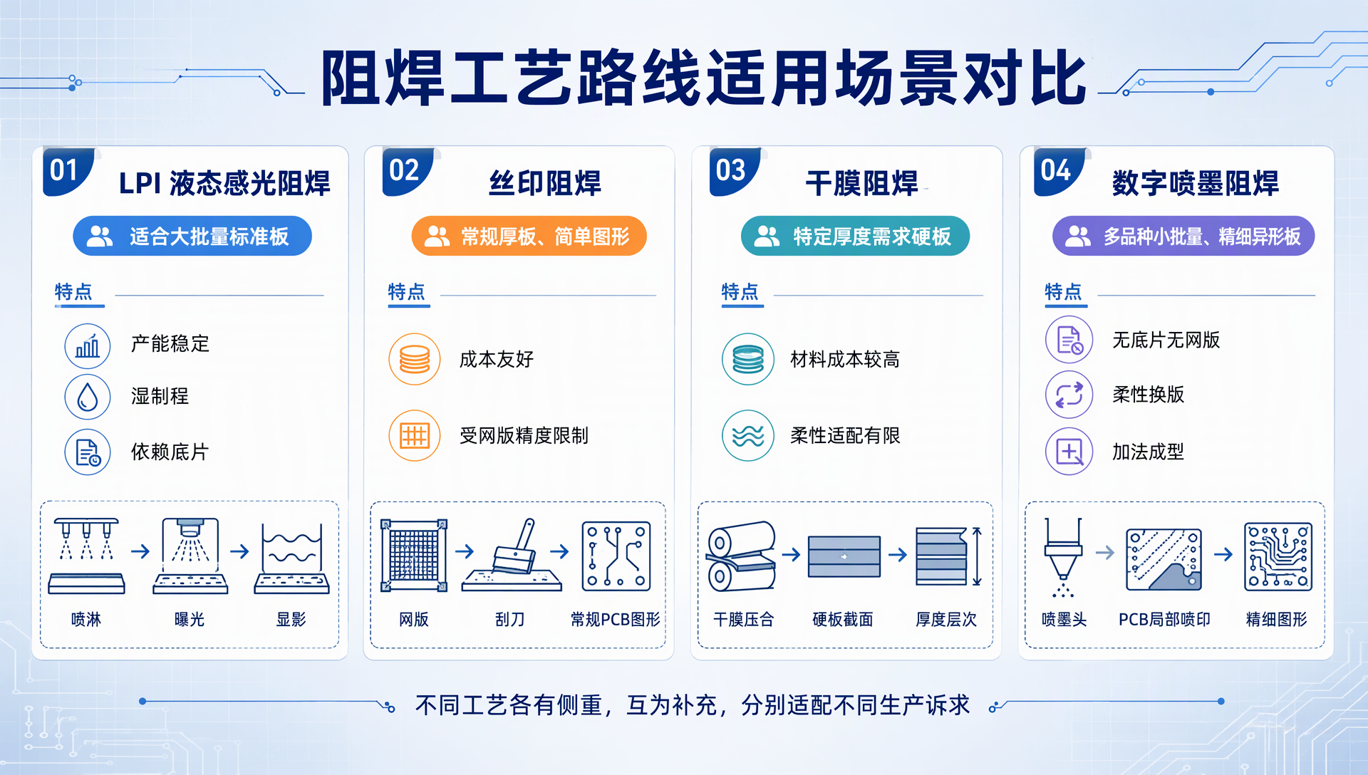
Digital inkjet solder mask is a differentiated digital process route that complements existing mature solder mask processes in the industry. Each is suited to different production requirements, with different strength scenarios:
(1)Liquid photoimageable (LPI) solder mask involves multiple steps including full-board spray coating, pre-baking, exposure, development, and post-curing. It relies on films and wet processes and is suitable for high-volume standardized board production, but it requires a large production footprint and longer changeover cycles, and in ultra-fine precision circuit processing it is prone to risks such as ink bleeding and residue. Screen-printed solder mask is formed by screens; registration accuracy has limits, making it difficult to meet ultra-fine circuit requirements, and its overall cost is not advantageous for small-batch orders. Dry film solder mask has relatively high material costs and a limited adjustable ink thickness range, with relatively limited adaptability on flexible substrates.
(2)Digital solder mask inkjet uses on-demand additive jetting to form solder mask patterns as needed, without films or screens, making it more suitable for multi-variety, flexible, and high-value-added production scenarios.
III. Core Value of the Solution
Hosonsoft PCB Solder Mask Ink Digital Inkjet Full-Stack Solution supports equipment OEM and integrator in rapid integration and solder mask inkjet complete-machine development. Relying on integrated collaborative control capabilities for inkjet, alignment, and curing, the solution delivers differentiated value from two dimensions: the PCB process side and the complete-machine development side:
(1) Process-side value: for PCB end factories
- No films or screens required; direct production from CAM graphics; flexible and efficient changeover; suitable for multi-variety mixed-line production models;
- On-demand additive jetting applies ink only to solder mask protection areas, improving consumable utilization;
- Eliminates wet process steps such as exposure and development, reduces waste liquid discharge, and aligns with green manufacturing trends;
- Controllable printed pattern edges and adjustable ink layer thickness ensure fine opening quality and reduce risks of ink bleeding and pad contamination;
- The production chain is simplified to pre-treatment—inkjet printing—UV curing, shortening the process flow and reducing production line footprint.
(2) Solution integration value: for equipment manufacturers and system integrator
- Achieves deep timing synchronization among inkjet, alignment, and curing, with control logic specifically adapted to the process characteristics of solder mask ink;
- Open architecture design supports matching and debugging with multiple printheads and UV solder mask inks, and supports customized development based on customer complete-machine requirements;
- Complete process support, with continuous ink matching and reliability DOE verification covering key indicators such as adhesion, reflow soldering resistance, chemical resistance, and insulation performance;
- Supports a joint development model, enabling synchronized joint debugging and testing with customers to collaboratively complete complete-machine process convergence.
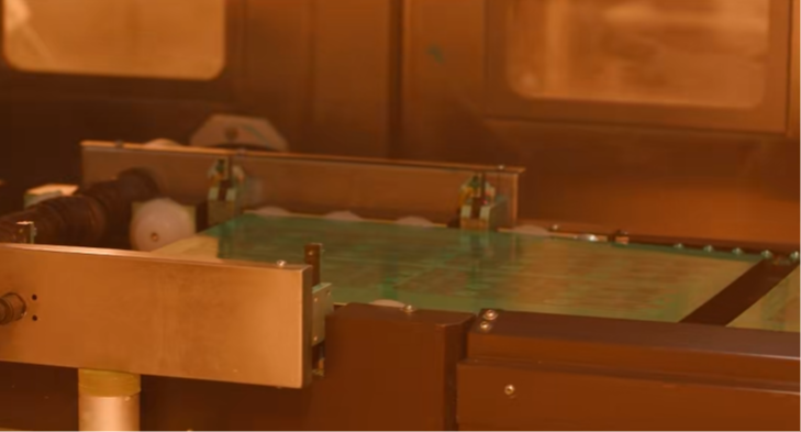
The digital upgrade of PCB inkjet manufacturing is moving from the "information layer" of character marking to the "functional layer" of solder mask ink. Solder mask inkjet is an important process direction for high-density, multi-variety production needs. Hosonsoft has been deeply engaged in industrial inkjet printing control for 20 years, continuously building industry experience and pursuing technological innovation. We look forward to working with industry partners to jointly unlock the value of digital inkjet in PCB solder mask processes!
For more details, please contact us.
 Back


