


 CN


Nanoimprint lithography (NIL), as an important alternative technology route to EUV lithography, is moving from laboratory research toward industrialization. The photoresist coating step is precisely a core bottleneck constraining NIL yield, per-wafer cost, and process window. This article will break down, layer by layer, the existing pain points of spin coating, the technical value of inkjet drop-on-demand, the process application boundaries, and the hardcore capability requirements for the control system, to clarify the core question: why the industry widely regards inkjet as the next-generation preferred solution for NIL photoresist coating.
I. The Role of Photoresist in NIL Scenarios and the Division of Industrialization Pace in the Track
Photoresist (photo-activated resist) is a core photosensitive material in micro/nanofabrication. It can undergo physicochemical changes under specific light exposure and, in combination with coating, exposure/curing, etching, and other processes, precisely transfer nanoscale patterns from a template to the surfaces of wafers and optical substrates.
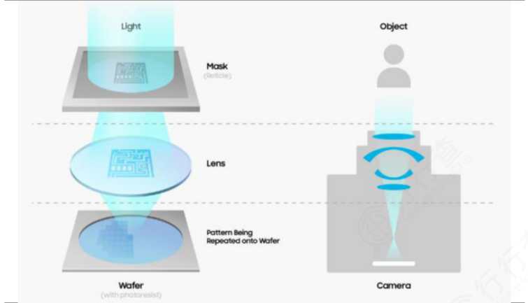
*Illustration: Schematic diagram of the photolithography process; Source: Xingxingcha (Samsung Semiconductor, Changjiang Securities Research Institute)
Tier 1: NIL nanoimprint and AR/XR optical waveguides
Grating regions have large variations in filling factor, devices are highly sensitive to residual layer thickness (RLT), and products iterate quickly; this is the direction where inkjet resist supply is first implemented and relatively mature in validation.
Tier 2: Selective coating for display panels and functional material deposition for advanced packaging
The core value comes from material savings on large-area substrates and precise deposition in local regions.
Target tier: Semiconductor front-end lithography
This is a stringent zero-defect scenario with an extremely long validation cycle; it is a long-term goal, not a short-term implementation track.
In short, inkjet photoresist is not a universal solution that can completely replace traditional processes. Its advantageous scenarios are concentrated in processes with uneven pattern density distribution, surface height structures, high photoresist unit cost, and strict material consumption control requirements.
II. Spin Coating Is Mature Enough; It Just Struggles to Match NIL’s Unique Requirements
Spin coating is a mature process validated over decades. In conventional scenarios with flat substrates and uniform film formation, it offers controllable thickness and a stable process, and it remains the industry’s mainstream choice today.
However, NIL has a notable characteristic: on the same substrate, template filling factors differ greatly across regions. This conflicts with the underlying logic of spin coating—“uniformly spreading resist across the entire surface”—which is what the industry calls the photoresist loading effect. Spin coating has two core pain points in NIL scenarios:
1. Low material utilization, driving up mass-production cost
Spin coating relies on centrifugal force to spread the resist; ultimately only 2%–5% of the photoresist remains on the substrate, and more than 95% is spun off as waste liquid. NIL imprint resists and high-refractive-index optical waveguide resists are expensive. In high-volume production, material waste directly raises per-wafer manufacturing cost and also brings additional pressure from waste-liquid treatment and environmental compliance.
2. Residual layer thickness cannot adapt, creating a yield bottleneck
Existing studies confirm that spin coating can produce a uniform resist film but cannot adapt to NIL templates with varying filling factors. Dense and sparse grating regions share the same resist layer thickness, causing inconsistent residual layer thickness after imprinting, directly interfering with subsequent etching and undermining nanoscale pattern consistency.
In addition, for high-aspect-ratio trenches, vias, irregular curved surfaces, and non-circular substrates, spin coating is prone to resist accumulation, local starvation, edge bead, and other defects, further narrowing the available process window.
Spin coating outputs a uniform-thickness resist film, whereas NIL truly needs dynamic resist allocation according to pattern requirements.
III. Inkjet Drop-on-Demand: The Next-Generation Solution for NIL Photoresist Coating
Inkjet drop-on-demand, in essence, turns photoresist into active digital dispensing: using picoliter-level droplets as the smallest unit, it dynamically calculates the required resist volume at each position based on local structural morphology, precisely controls droplet volume, landing position, and jetting density, and achieves “more resist for more filling, less resist for less filling,” actively compensating for loading effects.
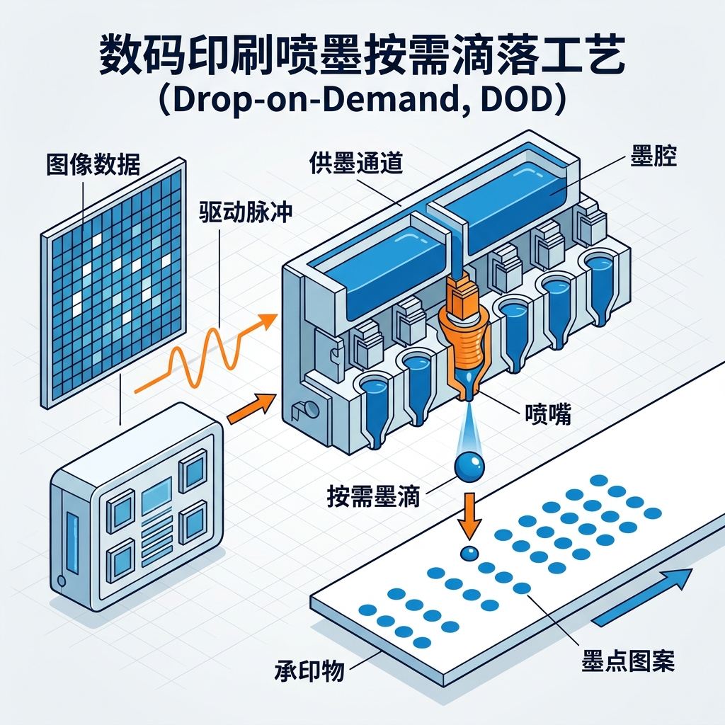
*Demonstration of the Principles of Digital Inkjet Printing
The underlying logic can be summarized in four points:
- Different resist thicknesses can be set in different regions of the same substrate so that the residual layer tends to be uniform across the entire imprinted area;
- Material is deposited only in areas that need imprinting, greatly improving material utilization;
- It adapts to curved surfaces, steps, and high-aspect-ratio structures, breaking through substrate-morphology limitations;
- Driven by digital patterns, changing templates or adjusting pattern density requires only modifying the jetting algorithm, without changing hardware tooling.
We must also objectively recognize the application boundaries of inkjet processes: inkjet itself has inherent process constraints. Thin-layer printing may suffer insufficient reflow and poor droplet coalescence, causing surface roughness defects; thick-layer printing tends to produce the coffee-ring effect; and when printing step structures, profiles tend to form slopes.
Inkjet is not a one-click universal replacement for spin coating. It is a systematic engineering effort requiring coordinated optimization of ink formulation, printhead selection, substrate surface pretreatment, and the underlying control system.
Photoresist Inkjet: Five Hardcore Capability Requirements for the Underlying Control System
How much value the inkjet process can ultimately release depends on whether the entire control system can handle complex operating conditions with multi-variable coupling. An inkjet system that stably adapts to photoresist must simultaneously possess five engineering capabilities:
1. Free waveform modulation capability for ultra-low-viscosity inks
Photoresist rheological properties vary widely, and low-viscosity UV-curable adhesives cannot be adapted with a fixed drive waveform; the underlying system needs to support custom waveforms and timing configurations, enabling hardware to adapt to material formulation iterations.
2. Picoliter-level metering to ensure long-term jetting consistency across multiple nozzles
Stable residual layer thickness is based on controllable volume of every resist droplet; in large-area array printhead scenarios, hundreds of nozzles must maintain consistent jetting volume over time, requiring independent-channel closed-loop metering.
3. Vision + motion + jetting closed-loop real-time compensation
Substrate warpage, deformation, and positioning offset can all cause droplet landing-position deviation; vision cannot serve as a post-hoc alignment tool, but must be embedded into the jetting trigger chain to achieve real-time compensation for position errors caused by substrate deformation.
4. Stable supply control for highly sensitive ink paths
Photoresist is highly prone to bubbles and sedimentation and is sensitive to temperature fluctuations; an ink path with temperature control, circulation, and degassing functions needs integrated debugging with the board and jetting timing so that faults can be quickly located and troubleshot.
5. Rapid multi-variable iterative validation capability
Pressure, drive waveform, and printhead temperature are strongly coupled; a high-quality underlying foundation must support rapid cyclic debugging to shorten the customer’s overall process development cycle.
IV. Solution Selection Approach: What to Focus on When Evaluating NIL Inkjet Solutions
At present, photoresist inkjet as a whole is transitioning from research prototypes to industrial equipment validation. For customers, the selection priority is not to look first for existing mature mass-production cases, but to judge whether the supplier can control the uncertainty in process introduction and keep risk within a manageable range. The core advantages of a full-stack self-developed solution are concentrated in two points:
1. Single point of responsibility, avoiding multi-party coordination disputes
If boards, vision, ink paths, and industrial control come from different suppliers, issues such as uneven residual layers, nozzle dropouts, and landing-position deviation can easily lead to mutual blame and slow root-cause location. With a full-stack integrated architecture, all modules are connected within the same system, enabling more efficient fault location and parameter debugging.
2. Transferable underlying capabilities, already validated in industrial scenarios
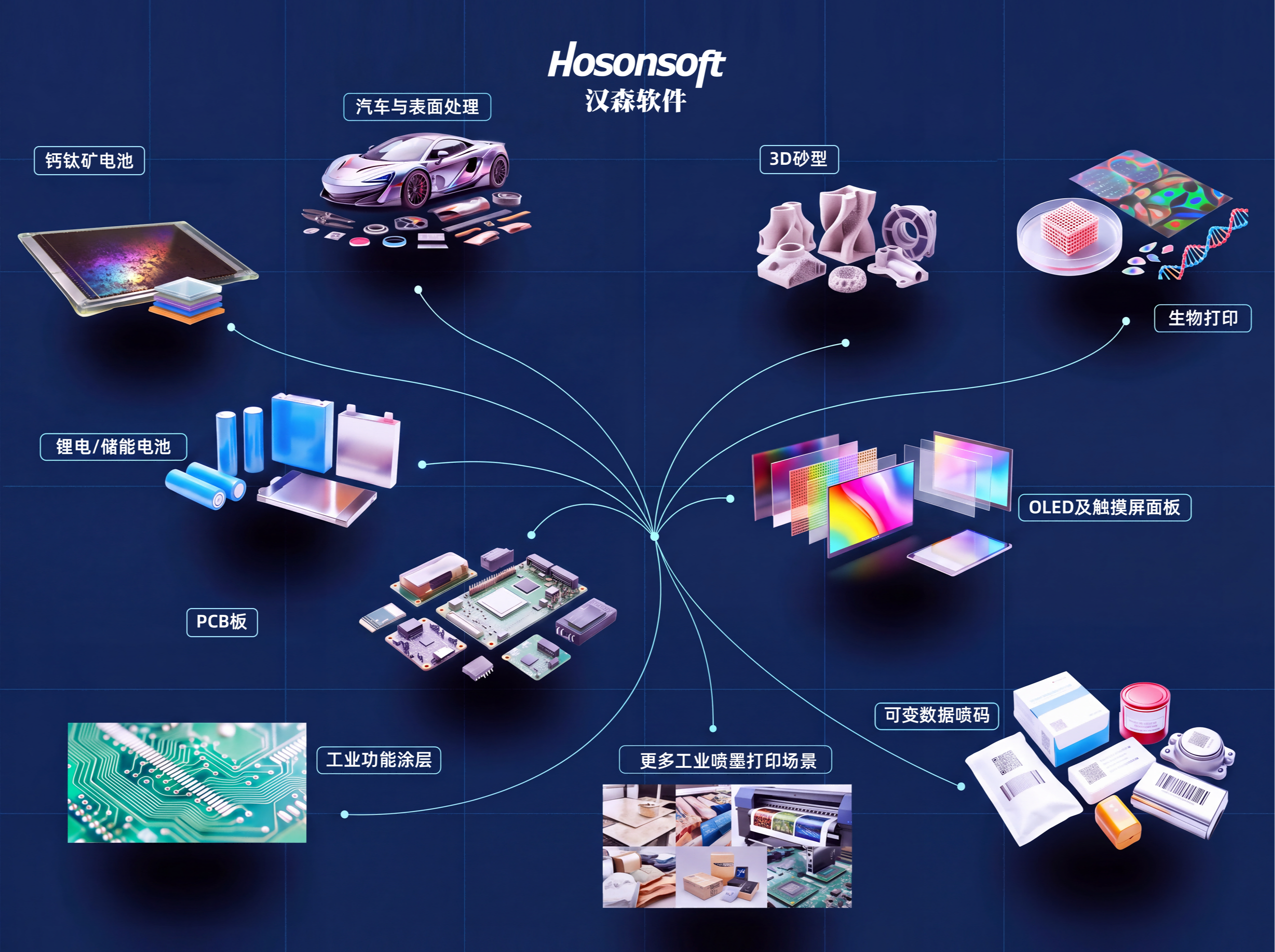
Scenarios such as PCB functional inkjet printing, new-energy battery cell insulation inkjet, and curved and irregular-surface printing also need to handle challenges such as deformed substrates, selective coating, and precise thickness control. The mature multi-printhead coordination, vision closed-loop, and ink-path control capabilities honed in these tracks are a reliable technology foundation for photoresist inkjet.

Spin coating remains a reliable solution for flat-substrate scenarios and will not be completely replaced. The core track for inkjet drop-on-demand is locked onto applications such as NIL, AR optical waveguides, and advanced packaging, where pattern density changes dynamically, structures are complex, and photoresist cost is sensitive.
As a micro/nanofabrication route with outstanding potential beyond EUV, NIL’s industrialization bottleneck has gradually shifted to: how to complete photoresist supply stably, at low cost, and in a controllable manner. Digital drop-on-demand is precisely the answer for the NIL coating step’s next-generation requirements. To implement this route, an industrially validated, fully connected inkjet control foundation is the prerequisite for all process iterations.
Shenzhen Hosonsoft Co., Ltd.
Founded in 2006, the company is a full-chain digital printing solutions provider in the industrial digital inkjet printing field. As the world's largest independent print control system supplier, it focuses on control systems, RIP software, SaaS platforms, and matching inks, building a full-industry-chain layout covering core components, software, cloud services, and consumables. The company holds more than 430 authorized patents, and its business covers more than 100 countries and over 20 industries worldwide. Its solutions have been widely implemented in textile, packaging, 3D printing, advertising, labels, lithium batteries, photovoltaics, semiconductors, biomedical, and many other industries. The company is committed to providing B2B customers with end-to-end, scalable, integrated printing solutions.
 Back


